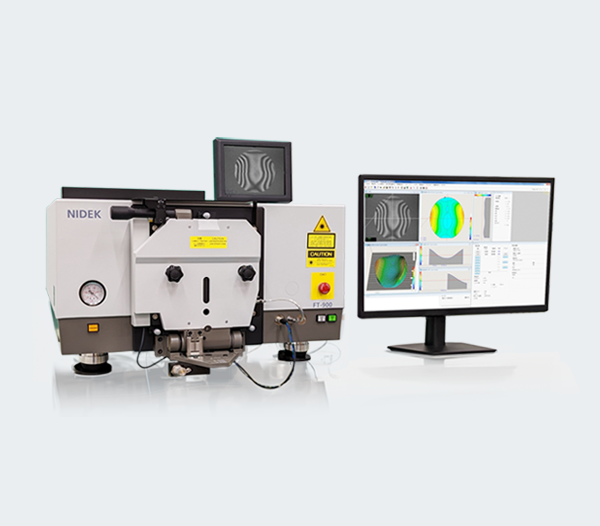
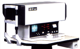
Flatness Tester
FT-17
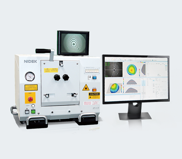
Slating incidence Interference method Flatness Tester
Features
- Samples up to outer diameter φ130 mm are measurable. (Up to φ100 mm for flatness measurement)
- Applicable to wafers (silicon, compound, oxide or glass), metallic fragments, disks (aluminum or glass), or user-defined shaped parts, etc.
- Applicable to mirrored/non-mirrored surface, transparent samples, perforated samples, or atypical samples
- Various samples are digitally measurable by analyzing interference fringe pattern obtained by laser oblique incidence interferometer through the phase shift method.
Detailed Information
Product information
- The measured data can be quickly acquired by full surface analysis with laser light.
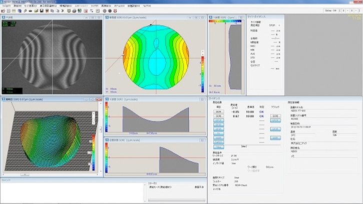
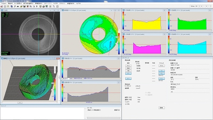
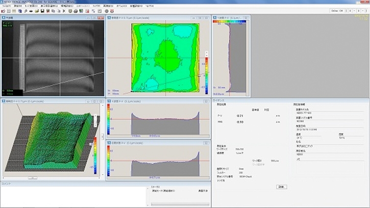
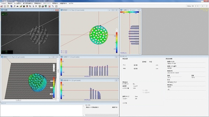
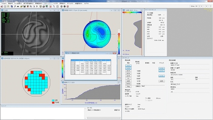
- The measurement result can be displayed as measured values, contour map, bird’s-eye view, cross-section view, etc.
- Original phase shift method is applicable to multiple interference fringes
- System control with exclusive analyzer running on the Windows platform provides easy operation.
- Transparent samples can not only be analyzed but also be measured with minimized interference of rear surface.
- The measurement result once obtained from sample data can be re-calculated to reflect changes in perimeter exclusion range, etc.
- Special calibration is unnecessary, pre-operation check with customer’s referential samples is recommended.
Abundant options
- Various software for each measurement of wafers, disks, square samples, user-defined shaped samples can be selectably used.
- Various Vacuum chucks for wafers enable High-precision GBIR (TTV) measurement
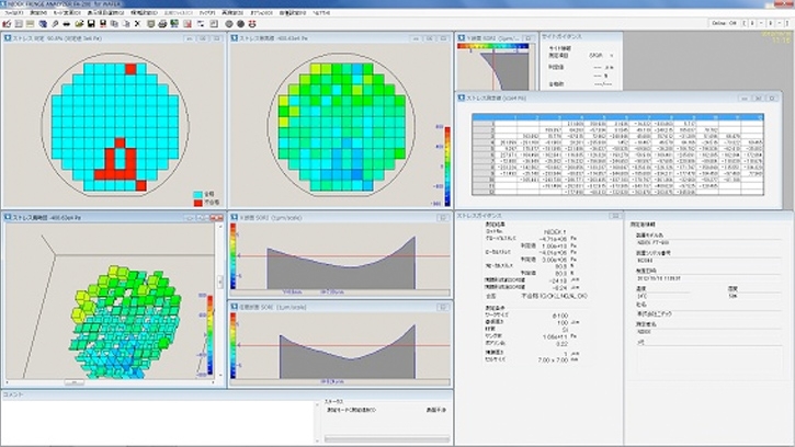
- Stepper simulation and Stress analysis software to meet the demands of wafers industry users
- Software for user-defined area enables partial measurement.
- Various types of cradles are available for each usage.
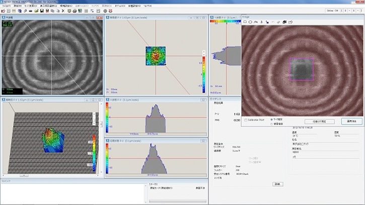
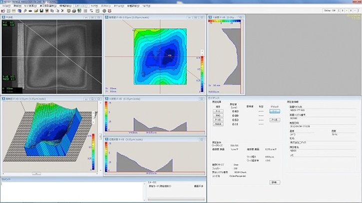
Sample of Displays
* Click to enlarge the image. Actual screens are displayed in English.
Specifications
| FT-17 series | FT-900 series | |||
|---|---|---|---|---|
| Without Fringe analyzer | With Fringe analyzer | With Fringe analyzer | ||
| Measuring method | Optical interference (Oblique incidence) | |||
| Light source | Semiconductor laser (655 nm, 3 mW) |
He-Ne laser (632.8 nm, 5 mW) |
||
| Sample size | Up to φ130 mm Up to φ100 mm for flatness measurement |
Up to φ200 mm | ||
| Sample thickness | Up to 10 mm (250 µm to 2000 µm for flatness measurement) Consultation available for requirements with other size |
|||
| Sample types | Wafer (silicon, compound, oxides or glass), Metallic fragments, Disks (aluminum or glass),Masks, etc. Mirrored or non-mirrored surfaces (excludes non-mirrored surfaces with low reflection) |
|||
| Sample tilt angle | Vertical or Vertical tilt at 8 degree angle | |||
| Interferometer sensitivity | 1, 2, 3, 4, or 5 µm/fringe (Only 1 or 2 µm/fringe on measurement with Lower surface reference,Data with 3 µm/fringe is reference) * Only 1 µm/fringe on measurement with Lower surface reference when Sample thickness is 1 mm or more. |
1, 2, 3, 4, 5,8 or 10 µm/fringe (Only 1 or 2 µm/fringe on measurement with Lower surface reference,Data with 3 µm/fringe is reference) * Only 1 µm/fringe on measurement with Lower surface reference when Sample thickness is 1 mm or more. |
||
| Rear interference sensitivity | —– | Varies depending on sample material (Example: For quartz, approx. 0.275 µm/fringe) |
||
| Measuring range | 30 times the size of Interferometer sensitivity (Actual value may be less, depending on fringe condition and zoom size etc.) |
|||
| Image magnification | 3x or higher (manual zoom) |
3x or higher (motorized zoom) |
||
| Display resolution | —– | 0.01 µm | ||
| Repeatability:1σ | —– | 0.02 S+0.02 M (µm) Condition: Setup sample uniformly then continuous measurement S = fringe sensitivity (µm) M = measured value (µm) |
||
| Effective pixels | —– | 640 x 480 | ||
| Measuring speed (OS Windows® platform without graphic display) |
—– | 6 sec or less | 6 sec or less (50 sec or less on simultaneous measurement with front & rear surface interference fringe) |
|
| Measurable area (Measurement may not be possible due to certain conditions.) |
—– | Whole area except 0.1 mm from the edges, Setting step: 0.01 mm |
Whole area except 0.1 mm from the edges, Setting step: 0.01 mm (On measurement with lower surface reference, the exception area becomes twice larger than the sample thickness, Setting step: 0.01 mm.) |
|
| Interferometer size (excludes protrusions) |
W521 x D485 x H438(mm) | W720 x D920 x H514 (mm) | ||
| Power source | AC100 V ± 10%, 50/60 Hz, 2.4 m length power cord with B type plug | |||
| 500 VA (FT-17 main unit: approx. 50 VA) | 600 VA (FT-900 main unit: approx. 100 VA) | |||
| Vacuum source | -80 x 10³ Pa or less, 20 L/min, 1/4 tube connection | |||
| Device configuration | Interferometer | Interferometer + Fringe analyzer (Personal Computer, 24 inch LCD monitor, one type of standard software,DVD±R/RW, Recipe function, Horizontal flip,Re-calculation function, 8.4-inch Interference fringe observation monitor) |
||
| Environmental conditions during use (Temperature, Humidity, Altitude) |
23 ± 3°C, 50 ± 20%RH (non-condensing) 2,000m or lower adove sealevel |
|||
| Weight | Interferometer(main body) : Approx. 90 kg |
Interferometer (main body) : Approx. 90 kg Fringe analyzer : Approx. 30 kg |
Interferometer (main body) : Approx. 140 kg Fringe analyzer : Approx. 30 kg |
|
| Fringe Analyzer software (Standard software is any one of Wafer, Disk, or Square, Others are option) |
Display function | —– | Interference fringe, Bird’s-eye view, Contour map, Cross-section view, Measured values, Measuring parameters, Map data, etc. |
|
| Wafer | —– | SEMI compliant (TV, GBIR, GFLR, GF3D, GF3R, SORI), BOW, Taper | ||
| Wafer OP | —– | Stepper simulation, Stress analysis All Sample Data and All Measurement Data(640×480) | ||
| Disk | —– | P-V, RMS, TIR, VEL, ACC (FT-17) | ||
| Square | —– | P-V, RMS | ||
| Square OP | —– | Stress analysis | ||
| Common OP | —– | Software for user-defined area (Noncompliant to Measurement for User-defined shape) | ||
| User-defined shape | —– | Software for User-defined shape: P-V, RMS | ||
Brochure Request
For inquiries and brochure requests, please contact the following URL.
Related Products
NOTE
The availability of products differs from country to country depending on the status of approval.
Specifications and design are subject to change without notice.
















 TOP
TOP
